


The UV additive manufacturing techniques discussed in prior columns have focused primarily on hardware approaches to additive manufacturing or the chemistry developed in combination with those approaches. 1 The current column is a brief survey of the use of UV additive manufacturing to enable and enhance the capabilities of artificial intelligence (AI). The subject of this column is not the use of AI modeling for molecular design or materials formulation development, but the use of UV additive manufacturing as part of the manufacturing process for the production of the advanced computational hardware itself. The challenges of this subject matter include its enormous scope and rapid growth. Many references that are only a year old contain statements and projections that no longer are valid. This column is intended to provide a brief overview of current growth opportunities for additive manufacturing in this rapidly developing area. Two key limiting factors for data center efficiency – networking speed and energy efficiency – are the focus of this discussion.
Networking Speed
Ethernet connections are the copper or optical fiber connections that link not only our homes, offices and the greater internet, including AI data centers, but also the processors within the data center. Hallmarks of an AI data center include the use of GPUs (Graphical Processing Units) for neural networks requiring high-throughput parallel processing with minimal delays in data transmission. A typical AI data center may contain 100,000 GPUs, and communication delays rapidly lead to decreases in system efficiency and increases in operating costs. 2
The trend is toward increasing link speeds for Ethernet networking. In many ways, the speed increases for data center networking are paralleling those that occurred over the last decades in single-processor computing, and 6.4 Tb (terabyte) communications already have been demonstrated.
Energy Demands
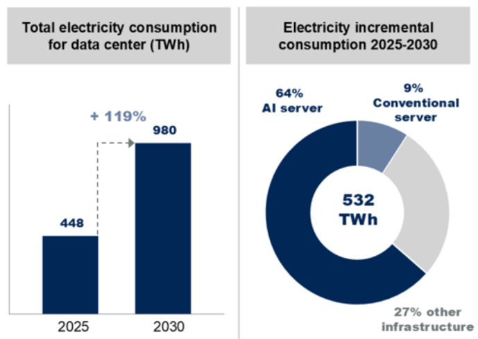
Concomitant with the increase in link speeds is the energy consumption to power the data centers themselves. With increasing numbers of GPUs in a smaller space, the power and cooling requirements continue to grow, contributing to the global trends shown in Figure 1. The individual regional impacts for the US, Europe and China are different due to factors such as server efficiencies and energy infrastructure, but the overall trends are clear.
As the line speed increases, the electrical resistance properties of copper reduce the maximum connection distance and increase the power requirements. In contrast, optical fiber requires less power and can transmit over longer distances. Network transmission is controlled by semiconductor switches that transmit and receive data between network devices. Increasing the line speed in and out of the switch increases the speed of the system and maximizes the processing capabilities of the GPU. The growing trend is a reduction in the length of the copper connections and an increase in the length of the optical connections to the point where the optics are directly adjacent to the switch die. By integrating the fiber communications into the device itself rather than using an external pluggable transmitter/receiver, the power requirements are reduced from 30 W to 9 W, a very significant reduction in heat generation and energy costs.
Photopolymer Additive Applications in Data Center Infrastructure
UV coatings have been utilized in the manufacture of optical fibers for over 40 years and continue to develop. 6 This column is focused on the use of micron-scale UV additive manufacturing co-packaged optics utilizing two-photon polymerization (TPP), a technique I have discussed in a previous column. 7 The benefits of TPP in CPO optics are very high spatial resolution and surface quality, leading to their use for in-situ manufacture of waveguides, waveguide couplers, lenses and lens arrays. 8
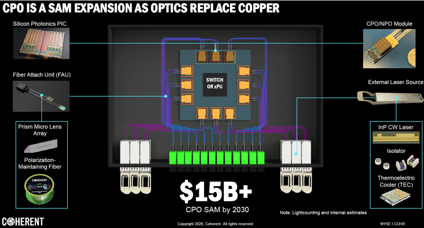
The details of a representative co-packaged optics (CPO) switch configuration broken down into its individual components are shown in Figure 2. The lenses and lens arrays that couple the optical fibers to the laser sources and silicon photonic circuitry are critical components of CPO hardware. The core of the device is silicon photonics, in which the signal is transmitted with light instead of as an electrical signal. Instead of losses due to resistance or impedance, the challenge becomes optical coupling loss.
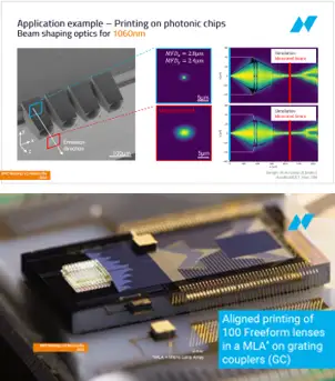
There are a range of designs for the optical coupling of chips. The two discussed here, free form and nanoimprint lithography (NIL), have been reported by Nanophase, a supplier of equipment and materials to the industry. The shape of the optical beam that couples the photonic chip to the optical waveguide is achieved by precise control of the shrinkage of the resin during cure, the refractive index at the specific laser wavelength and the surface roughness (Figure 3). The freeform optic shown on the left is used to generate a precise beam shape that closely matches theoretical models. The optic on the right consists of an array of 100 microlenses printed on a grating optical fiber coupler.
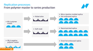
NIL can involve the 3D printing of a positive master, which then is used to create a negative mold that can be microinjected with optical resin or used for hot embossing or nanoimprinting. Alternatively, NIL can utilize a 3D-printed negative master which is then used for embossing directly. In both cases, the printing of the masters does not require that the 3D material be optically transparent, but rather only that it provides the correct thermomechanical and surface properties to support the embossing process. Examples of NIL are shown in Figure 4.
The need for more energy-efficient, high-speed photonics will continue to grow in support of the rapidly expanding demand for AI data center capacity. As the dimensions of photonic devices continue to decrease and the density of devices in data centers continues to increase, UV additive techniques such as two photon polymerization support the growth of the photonics industry.
For feedback, or if there are specific topics readers would like to see discussed, please feel free to contact me at pshare@admatdesign.com.
Resources:
- This column is focused on photopolymer applications in additive manufacturing in which a reservoir or vat of liquid resin is photopolymerized to generate a part. When a layer is cured using a narrow laser beam in a series manner, one point at a time, it is referred to as stereolithography or SLA. Simultaneous illumination of a large area to cure one full layer at a time can be accomplished with a digital light projector or DLP or a liquid crystal display (LCD) screen.
- https://developer.nvidia.com/blog/making-gpu-clusters-more-efficient-with-nvidia-data-center-monitoring/ (Accessed 7/10/2026)
- 2026 Ethernet Roadmap. The Past, Present, and Future of Ethernet Ethernet Alliance, February 2026
- https://www.gartner.com/en/newsroom/press-releases/2025-11-17-gartner-says-electricity-demand-for-data-centers-to-grow-16-percent-in-2025-and-double-by-2030 (Accessed 7/10/26)
- https://developer.nvidia.com/blog/scaling-ai-factories-with-co-packaged-optics-for-better-power-efficiency/ (Accessed 7/8/26)
- Janani, R.; Majumder, D.; Scrimshire, A.; Stone, A.; Wakelin, E.; Jones, A.; Wheeler, N.; Brooks, W.; Bingham, P. From Acrylates to Silicones: A Review of Common Optical Fibre Coatings used for Normal to Harsh Environments Progress in Organic Coatings, 2023, 180, 107557-107569
- Share, P. Advances in Photopolymer Design UV+EB Technology, 2026, 12(2), 18-19
- Weninger, D.; Serna, S.; Ranno, L.; Kimerling, L.; Agarwal, A. Advances in Waveguide to Waveguide Couplers for 3D Integrated Photonic Packaging Light: Science and Applications, 2026, 15:17, 1-49
- Coherent Technology Innovation Briefing, March 17, 2026
- Smolenski, J. From Mastering to Aligned Printing – Enabling Photonics Systems Production with 2GL Epic Technology Meeting on Microelectronics and Photonics, November 14, 2023

Paul Share, Ph.D.
Principal Consultant
Advanced Materials Design LLC