

By Jennifer Heathcote, Eminence UV
The list of viable UV LED applications continues to grow – as does the number of system suppliers, formulators and OEM machine builders supporting those applications. This ongoing increase in activity bodes well for the general market direction of UV LED technology. As a result, those who aren’t already investigating its suitability for their own curing needs may find it is time to start. For newcomers, as well as those who have been following or even using the technology for years, this paper is meant to provide insight into the growing UV LED market space and to offer general guidance regarding how to match a UV LED curing system to the needs of a given application.
UV output
UV output is characterized by wavelength (nm), irradiance (W/cm2) and energy density (J/cm2). Understanding how these three components interact with UV LED-formulated inks, coatings and adhesives under specific manufacturing conditions is essential to developing and ensuring successful and controllable curing applications. A key advantage of UV LED curing is that once the optimal combination of these three components is established for a given application, a properly matched and suitably designed UV curing source will provide consistent, reliable and repeatable UV output over time.
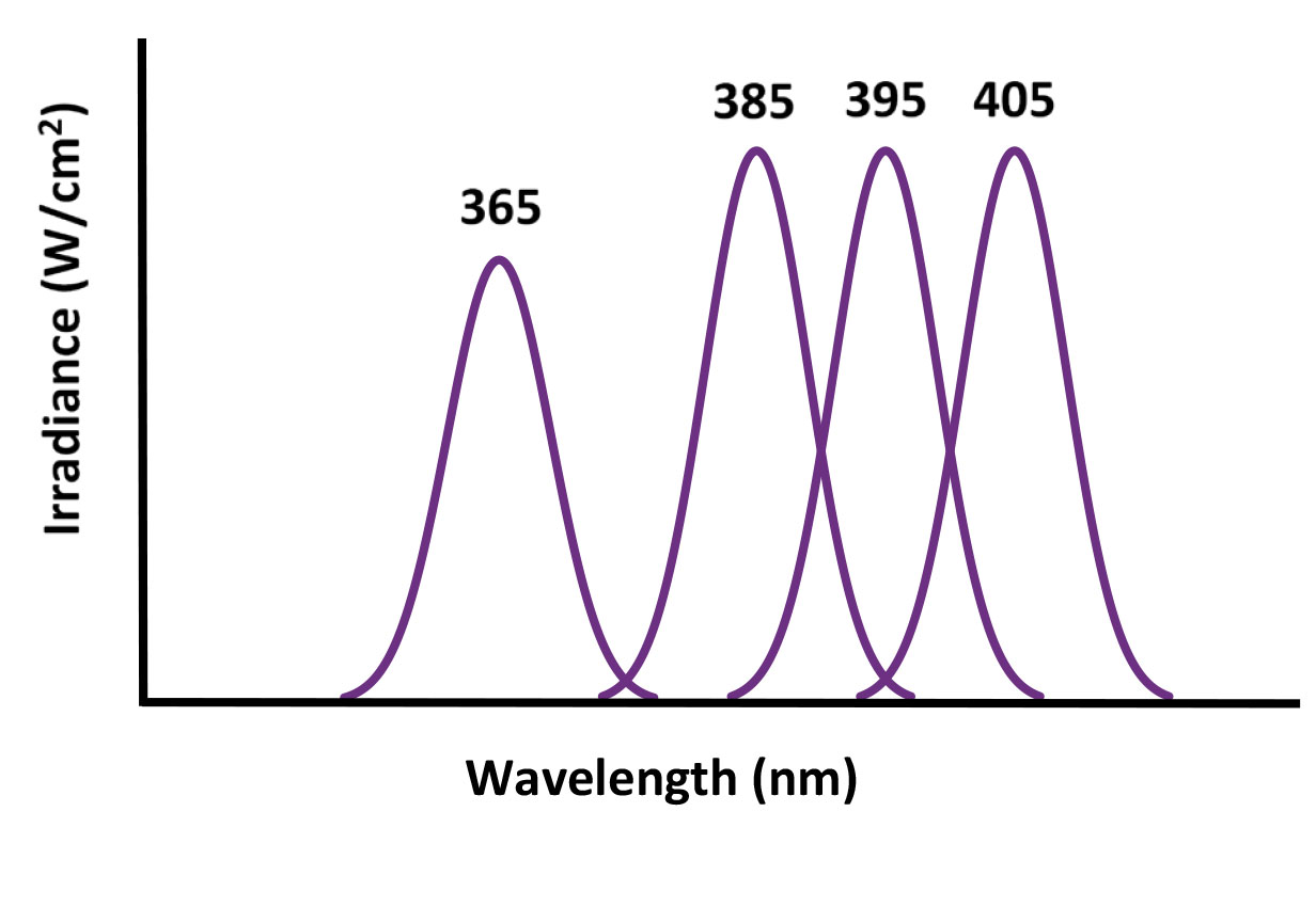
For UV LED systems, the emitted wavelengths are relatively monochromatic and represented by narrow, bell-shaped distributions with nominal peak irradiances currently at 365, 385, 395, and 405 nm, as shown in Figure 1. The exact wavelength where the peak occurs, as well as the shape of the distribution, is entirely dependent on the raw diode’s material structure and is not adjustable after the diodes are fabricated. While two or more distributions can be blended within a single UV LED device, most curing systems typically incorporate just one. Due to its different material structure, and identified by the shorter peak in the graph, the maximum irradiance at 365 nm currently lags the three longer wavelengths by roughly 20%.
Unlike peak wavelength, both irradiance and energy density are highly variable components of UV LED output. The respective magnitudes at the emitting window, as well as at the cure surface, are driven by numerous factors in the overall lamp head design. Irradiance and energy density vary significantly across product models, often are adjustable for a given system and are highly impacted by the installation set-up. The advantage of this variability is that it allows users to precisely and efficiently optimize manufacturing processes.
For UV LED curing systems, peak irradiance should not be used as an indicator of energy density in dynamic manufacturing processes. Instead, both values should be specified by the supplier and/or measured. Other data points matching the desired manufacturing conditions can then be extrapolated. The measurement device, set-up and method of data collection always should be referenced when reporting irradiance and energy density, as all three impact the observed values.
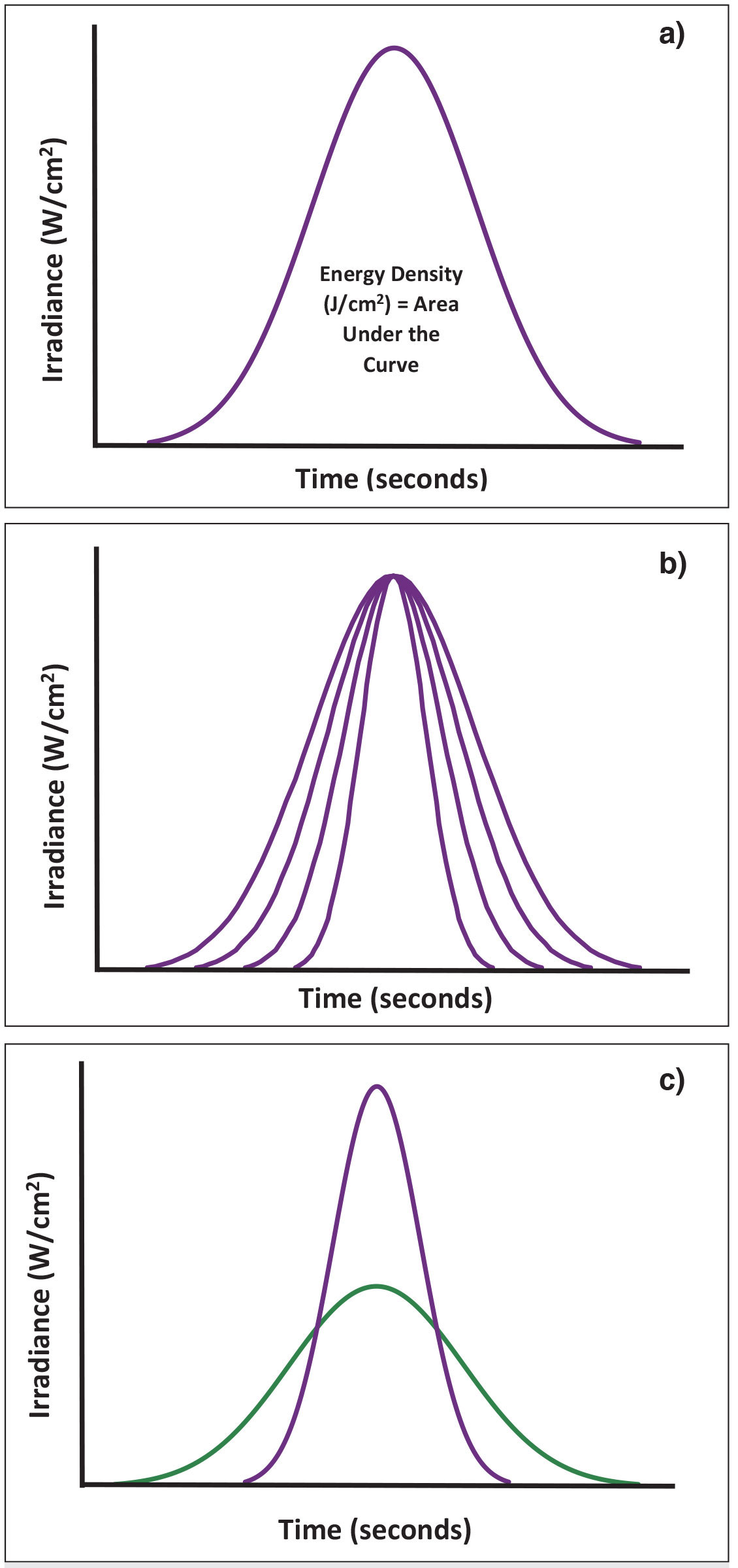
For clarity, irradiance is the peak power, and energy density is the total delivered energy. In mathematical terms, energy density is the integral of irradiance over time and is represented by the area under the irradiance vs. time profile. Figure 2(a) is a graphical illustration of a point on a cure surface moving horizontally (along the x-axis) under the perpendicular length of a UV LED lamp at a fixed working distance over time. Each point on the curve is the irradiance that the cure surface experiences at each moment in time, and the area under the curve is the total emitted energy density. UV LED systems with the same peak irradiance do not always deliver the same energy densities, as shown in Figure 2(b).
Note that the areas under the four separate profiles in (b) are not identical. The outermost profile with the greater area delivers the most energy density and the innermost profile the least. Two systems with dissimilar irradiances also can deliver the same total energy density, as demonstrated by Figure 2(c). One curve has a peak irradiance that is half of the other; however, the areas – and therefore the energy densities – are identical. One difference in lamp head design that would produce this result would be for the taller peak to have an emitting window width that is half the width of the shorter peak. These three examples illustrate the importance of understanding the impact of both the emitted and delivered irradiance and energy density when matching a UV LED system to the application as well as why not all UV LED systems behave identically in a lab set-up or commercial installation.
Inks, coatings and adhesives are formulated to react to a given UV LED output under a specific set of process conditions. For each application and formulation, there is a UV process window within which acceptable cure can be achieved. This window is not narrow, but there is an optimal set of wavelengths as well as a minimum and maximum irradiance and energy density combination that results in proper cure. Consistently operating within this window better ensures optimal line speed, a non-tacky surface, adequate adhesion, sufficient cure, minimal post-cure migration and desired product life, among other desired performance criteria. Establishing and maintaining a UV process window for a given application is important for producing optimal yields and quality product over time.
UV LED technology performs well when UV output is correctly matched to the needs of the application and paired with a suitably formulated ink, coating or adhesive. Unfortunately, there is no universal UV LED system or process window that works equally well for all applications. The UV LED solution and its output should be chosen for the formulation, the plant or shop environment, and the configuration and speed of the material-handling system.
A benefit of UV LED technology is that the discrete nature of LEDs allows for a much wider range of curing system designs that can better fit the needs of each unique application. This allows both form factor and UV output to be tailored to the respective markets and applications, resulting in much more efficient and economical UV LED curing solutions as compared with conventional curing technology.
Application evolution
UV digital inkjet pinning and full-cure for scanning and single-pass printers, as well as spot-cure adhesive lines, were the first applications to adopt UV LED curing into printing and bonding processes. Many of the early installations were hybrids that utilized some aspect of conventional curing in conjunction with UV LED. These early adopter markets capitalized on slower line speeds and longer part processing times to successfully enable UV LED technology during the mid-2000s. Manufacturing methods allowed energy density to build through longer exposure times in static installations and through multiple passes in dynamic ones. Set-ups also provided the ability to mount the UV LED heads within 10 mm of the cure surface and typically had lower requirements for the total number and length of lamps per machine. The need for only one or two smaller lamps resulted in a lower commercial investment compared to that of larger and wider high-speed commercial presses. All these factors were crucial, as early UV LED systems were not very powerful and often were more expensive than conventional options.
Over the past 15 years, UV LED technology has improved dramatically in terms of performance, reliability, life and output. In addition, many more formulations have been optimized for UV LED output, the market has learned to understand and engineer to the process window, and the price points of equipment and formulations have improved due to economies of scale and more competition throughout the supply chain. This has allowed UV LED curing technology to move beyond UV digital inkjet pinning and spot cure into more demanding, higher speed and wider commercial applications – both analog and digital.
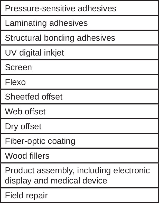
Table 1 represents areas where UV LED technology is increasingly being used today – albeit at varying levels of market penetration and not necessarily for all applications within each market segment – but that will continue to improve with time. Different UV LED lamp designs, as well as application-specific formulations, are needed to make these diverse printing, coating and bonding processes feasible. As a result, it is important that, for each application, there be a strong working relationship among all parties – UV LED curing system supplier, formulator, OEM machine builder, integrator and end user. In all cases, a viable UV LED solution typically can be achieved with some trial and error, and process optimization. It all comes down to identifying the process variables and matching the UV LED system to the application, formulation and material-handling equipment.
Matching UV LED systems to the application, formulation and material-handling equipment
There is an ever-increasing abundance of UV LED curing systems and vendors from which to choose. All claim very similar product features and operational benefits, with the most obvious differentiators being the peak irradiance, cooling method and lamp form factor. Unfortunately, knowledge of these alone is insufficient for matching UV LED curing systems to a given application, and technical spec sheets rarely provide explanations as to which product(s) are best suited for a given application and why. When matching a UV LED curing system, the following general guidelines should be considered.
Final Cure Properties
The desired physical and aesthetic properties of the final cure as well as the intended product use should be specified and are instrumental in driving the formulation chemistry and, ultimately, whether a UV LED cured solution is even possible today. For example, inks, varnishes and adhesives generally cure well with LED and meet most graphic print requirements. Silicone release and industrial hard coats, however, still are very much in development and are at least three to five years away from wide-scale commercial availability.
Wavelength
Commercial curing wavelengths currently include 365, 385, 395 and 405 nm. For most ink applications, 395 nm is the preferred wavelength, with 365 and 385 nm wavelengths used to a lesser degree. Adhesives typically work best with 365 or 405 nm, depending on the formulation, but also cure similarly with 385 or 395 nm. Overprint varnishes tend to match the ink wavelength of 395 nm, and when it comes to industrial coatings – both functional and hard – there is no consensus, as development still is very much in its infancy.
Irradiance Window
The formulation chemistry must be cured within a minimum and maximum peak irradiance (Watts/cm2). Operating below a minimum irradiance will result in insufficient cure, and increasing irradiance beyond the maximum does not necessarily produce better results than curing within the established irradiance window, provided the lamp emits enough energy density. Unfortunately, there is no universal irradiance that meets the needs of all formulations. Each application is different, with the optimal emitted irradiance window spanning anywhere from a few hundred mW/cm2 up to 20 or even 30 Watts/cm2. More important than the emitted irradiance, however, is the actual irradiance that is delivered to the substrate cure surface, as irradiance decreases quickly with distance traveled.
Energy Density Window
The formulation and the manufacturing line speed determine the necessary energy density (Joules/cm2). A greater energy density generally results in a better overall cure, allows for a faster line speed and sometimes enables a lower peak irradiance. Not all systems emitting the same peak irradiance deliver the same energy density. Energy density can be increased by using a lamp which, by design, emits greater energy density, using multiple lamps in combination, slowing the line speed, or increasing exposure time.
Working Distance
This is defined as the offset between the UV LED emitting window and the cure surface. It must be specified for the application and machine set-up, as irradiance decreases quickly with distance. To accommodate greater working distances, consider more powerful lamps (either greater irradiance, greater energy density or both) or an LED solution that incorporates optics or reflectors.
Cooling Mechanism
The plant environment, preference of the OEM or end user and UV LED system design determine the cooling mechanism (air or water). Not all UV LED products are available in air-cooled variations, and higher-powered systems are typically water cooled.
Mounting Space
The mounting location and machine set-up determine the allowable space for the UV LED head. Water-cooled systems are generally more compact than air-cooled systems. Air-cooled systems also require a minimum clearance around both the air inlets and outlets to ensure adequate circulation.
Optics and Shielding
The lamp proximity and orientation to unwanted cure surfaces influences the use of optics and shielding. Care should be exercised to ensure that UV rays are blocked from digital inkjet print heads, ink and coating pans, and heat-sensitive materials on the machine. In addition, all light should be shielded from any direct line of sight with the operator.
Drastic Part Profiles
Industrial applications with drastic part surface profiles, cure surfaces or manufacturing lines that require the LED lamps to be mounted at a greater distance (several inches or more), and the need for incredibly hard, scratch and chemical resistant UV LED top coats still are a bit of a challenge and should be considered in-development for the foreseeable future.
While there will continue to be ongoing development for years to come, UV LED curing technology is certainly finding a home in a growing number of applications. Despite the inability to use the exact same system interchangeably across the previously shown list of applications, there do exist unique UV LED solution sets that meet the needs of many applications. While OEMs may perform the LED curing device and formulation matching for buyers ahead of purchase, it is always recommended that users confirm through testing or by referencing previous installations that the correct system was indeed matched to the specific needs of the process. Follow the guidelines in this paper and work closely with the UV LED curing system suppliers, formulators, OEM machine builders, integrators and end users to ensure greater overall UV LED curing success.
Jennifer Heathcote, Chicago, Illinois, has been in the UV equipment and applications business since 1998. She is a technical and commercial consulting adviser with Eminence UV and also serves as an executive board member for RadTech North America. Her roles in the UV industry have included applications engineering, sales, business development and general management. She has presented at numerous conferences and industry events, authored nearly two dozen articles on the subject of UV curing and, in 2012, co-authored The UV LED Handbook. She earned a BS in mechanical engineering from Purdue University and an MBA from The Ohio State University.


