

By Liz Stevens, writer, UV+EB Technology
The performance of modern optical devices – from extended reality headsets to organic light-emitting diode (OLED) displays and precision sensors – depends on the ability to precisely control how light behaves as it moves through layered materials. Refractive index, the measure of how much a material bends light, is a foundational parameter in optical design, governing everything from field of view in a waveguide to light extraction efficiency in an emissive display. Achieving the refractive index values required for today’s demanding applications calls for advanced materials engineered at the nanoscale, where the size and composition of particles can be tuned to deliver specific optical properties with consistency and repeatability. Nanocrystal-based formulations have emerged as an enabling technology in this space, giving manufacturers of optical components and displays a new level of control over the materials that shape how their devices perform.
Pixelligent Technologies LLC, Baltimore, Maryland, specializes in material technology for advanced optical and display manufacturing. The company’s formulations feature tunable nanocrystal-enabled formulations for nanoimprint lithography, micro-imprinting and inkjet printing, yielding structured optical layers with high refractive indices for guiding and bending light as it passes from one medium to another. Neil Pschirer, vice president of product and strategy, provided insight into the company’s materials and their value in optical and display applications.
Refractive Indices

Pixelligent offers materials with refractive indices ranging from 1.6 to over 2.0 across the visible spectrum (380-700 nm), with standard measurements taken at 589 nm, to facilitate control of light capture, light extraction, light throughput and field of view. These materials are used as optical layers in extended reality devices (XR), displays, sensors and OLEDs (Figure 1). When used in XR devices, the company’s optical film widens the field of view in waveguides for a more immersive visual experience for users. In MicroLED displays and OLEDs, formulations with high refractive indices improve light extraction for greater brightness, enhanced device efficiency and prolonged device lifetimes. Higher refractive indices in optical sensors deliver enhanced light capture and throughput, improving sensing precision, accuracy and range.
UV as an Enabling Technology
UV plays a dual role in these material systems, both in processing and in long-term performance. “Our nanocrystal formulations are designed for UV-curable processes, such as coating, inkjet printing and nanoimprint lithography,” said Pschirer. “UV exposure enables rapid curing and pattern transfer, supporting high-throughput manufacturing and compatibility with temperature-sensitive substrates, including plastics used in XR and sensor applications.” The materials typically are cured at 365 nm; however, the cure wavelength can be shifted to lower energy for applications, such as OLED.
In addition, the company’s materials are engineered for UV stability and long-term performance. “Maintaining optical clarity, refractive index and low haze under prolonged UV exposure,” Pschirer said, “are critical for applications such as XR headsets, automotive displays and optical sensors, where sustained illumination can impact device performance.”
Guiding and Bending Light
The company’s products and the tunable nanocrystals, central to the formulations, produce optical layers with a variety of light-manipulating qualities. “For light capture, such as time-of-flight (ToF) sensors,” said Pschirer, “our PixMicro™ formulations can be used to improve sensing efficiency through patterned high-index diffusers.” In OLED displays, the materials are used to enhance light extraction by improving the coupling of light out of the device. “In applications such as ophthalmic lenses,” Pschirer said, “our materials support high refractive index and high optical transmission with low haze, reducing the size and weight of lenses with minimal scattering loss.”
Extended reality (XR) devices benefit from high-index nanocomposites that enhance light propagation within waveguides, enabling wider field-of-view designs with improved efficiency. “In XR waveguides,” Pschirer explained, “nanostructured diffractive gratings produced with our formulations couple light into high-refractive-index substrates, where it propagates via total internal reflection (TIR) before being extracted to the viewer as a virtual image. Precise control of refractive index is critical to maintaining efficient TIR and ensuring effective light guidance through the waveguide architecture.”
Products and Applications
Pixelligent has several types of nanoparticle dispersions which enable a wide range of refractive indices. Its PixClear® Designer Compounds® category includes Titania and Zirconia dispersions. Titania is a class of ultra-high refractive index (HRI) dispersion materials that are available in sizes from 10 nm to 20 nm capped nanocrystals. The Zirconia dispersions are composed of sizes from 3 nm up to 10 nm capped particles. These nanocrystals enable customers to achieve exceptional optical performance and robust mechanical properties and are suited to expand the field-of-view in extended reality devices, boost the light output in OLED and MicroLED displays, deliver sharper images in optical sensors and enable high-performance 3D-printed optics.
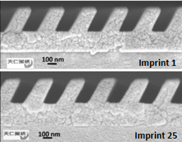
PixCor® is a proprietary core-shell design created by the company’s nanotechnology scientists that can be used to passivate its Titania core with a Zirconia shell, delivering UV stability, high-refractive-index, low haze and high transparency for superior optical fidelity and image quality in pass-through optics applications. This core-shell technology underpins three categories of formulations based on application technique. PixNIL® is a solvent-based formulation designed for nanoimprint lithography (NIL). It is suited for extended reality (XR) and metalens applications. “With nanoimprint lithography,” said Pschirer, “these materials enable high-fidelity replication of subwavelength grating waveguide structures for XR displays based on surface relief gratings (SRG), maintaining feature definition across repeated imprint cycles. The result is a low-cost and scalable replication. For thin-film coatings, the materials can be applied through processes such as spin coating to form high-index optical layers used in XR systems or anti-reflective coatings” (Figure 2).
Solvent-free PixMicro™ formulations deliver material options optimized for next-generation applications. These formulations feature a range of refractive indices and viscosities for use in displays and sensors. They enable high-performance micro-imprinted microlens arrays for sensors, diffractive optical elements and light guides. Refractive indices from 1.65 to 1.9 are available, as well as customizable viscosities. It can be used with micro-imprintable products – glass and plastic substrates – and with commercially available microimprint stamps. “In micro-imprinting, these materials can be used to form microlens array structures for light shaping and optical efficiency improvements,” Pschirer said. “And with 3D printing or molding, precision ophthalmic/optical lenses of 1 mm or higher thickness with low coloration and low haze can be manufactured.”
The company also has inkjettable formulations that are solvent-free and have low viscosity (ca. 20 cP). These formulations are used mainly in OLED displays and can increase the light extraction of a display by up to 40%. “PixJet® formulations are designed for inkjet processing, enabling controlled deposition of high-index materials for OLED device structures,” said Pschirer. “In particular, our solvent-free inks can be deposited at the subpixel level in a simple two-step process, jet and cure. The alternative process, photolithography, is an expensive multistep approach with increased material waste.”
These product lines offer a materials tool kit engineered for the optical precision of extended reality devices, displays and sensors. Whether the goal is widening the field of view in an XR waveguide, boosting light extraction efficiency in a MicroLED or OLED panel, enhancing sensing accuracy through higher light capture or enabling scalable nanoimprint and inkjet manufacturing processes, the company’s tunable nanocrystal formulations address the performance requirements at the heart of each challenge.
Pixelligent welcomes inquiries from potential customers and partners working in advanced optics, coatings and high-throughput manufacturing. In particular, the company is interested in connecting with organizations exploring new applications for high-index materials, including XR, sensing and waveguide-based systems, where material performance directly impacts device efficiency and scalability.
Pixelligent Technologies is a RadTech 2025 RadLaunch awardee. For more information, visit www.pixelligent.com.