
By Stacy Hoge, marketing manager, Excelitas
UV and UV LED curing technologies are foundational to modern electronics manufacturing, enabling fast, precise and low-temperature bonding, sealing, coating and protection of sensitive components. Their rapid cure times, minimal thermal load and high repeatability make them essential for high-density, thermally constrained assemblies. UV curing is widely deployed across the production of artificial intelligence (AI) data-center hardware, semiconductor packaging, display and mobile device modules, optical films, PCBs and fiber-optic and cable assemblies. It also supports high-resolution printing for component identification, traceability and security features on optical and electrical cable films used in high-security infrastructure.
As AI infrastructure scales at an unprecedented pace, UV curing is emerging as a critical process in data center manufacturing. It enables fast, controlled hardening of adhesives, coatings and encapsulants without introducing thermal stress to tightly packed, high-power electronics. This broader infrastructure boom also is fueling rapid growth in multi-mode fiber-optic cable production, driven by the need for higher-capacity data pathways throughout AI facilities.
UV curing also plays a key role in the production of high-capacity Hard Disk Drives (HDDs), which remain the backbone of large-scale AI storage architectures. Solid State Drives (SSDs) have a limited life compared to HDDs, which makes HDDs well suited for long-term and archival data storage. Spot curing systems and custom light-delivery solutions are used widely in the manufacturing of HDDs and HDD components, particularly HDD head assemblies. During HDD manufacturing, UV spot-curing enables fast, controlled hardening of adhesives and coatings used in head-stack assemblies, actuator components, spindle motor subassemblies, and internal seals, all without introducing thermal stress to ultra-sensitive electromechanical parts.
UV Curing System Architectures

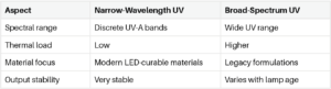
UV curing systems generally differ by system architecture (spot curing vs. area curing, Table 1) and by spectral output (narrow-wavelength vs. broad-spectrum UV, Table 2). These differences directly impact material compatibility, process design and thermal performance.
UV Spot Curing
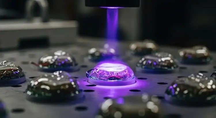
Spot curing systems are designed to deliver UV energy to a small, localized area with high precision. These systems typically use focused optics or light guides to direct UV radiation to a specific cure site.
Spot curing systems are commonly used for the following:
- Localized adhesive bonding
- Component attachment and wire tacking
- Connector and sensor fixation
- Optoelectronic assembly
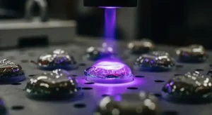
The primary advantage of spot curing is precise control of UV exposure while minimizing unintended irradiation of surrounding components (Figure 1).
UV Area Curing
Area curing systems emit UV radiation over a larger surface area, making them suitable for curing coatings or adhesives across entire assemblies or circuit boards. These systems frequently are integrated into inline conveyor processes to support high-throughput manufacturing.
Application descriptions indicate that area curing systems are used for the following:
- Conformal coating of electronic assemblies
- Potting and encapsulation
- Large adhesive bonds
- Inline curing in automated production lines
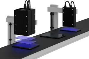
Area curing systems emphasize uniform irradiance distribution across the emitting window to ensure consistent curing over the full exposure area (Figure 2).
Spectral Output Comparison: Narrow-Wavelength vs. Broad-Spectrum UV
Narrow-Wavelength UV LED Sources
Narrow-wavelength UV systems emit light within a tightly controlled spectral band, typically in the UV-C and UV-A regions, with common emission peaks at 275, 365, 385, 395 and 405 nm (Figure 3). These wavelengths are intentionally matched to the photoinitiators used in modern UV-curable adhesives, coatings and inks, ensuring efficient energy absorption and reliable curing performance in electronics manufacturing.
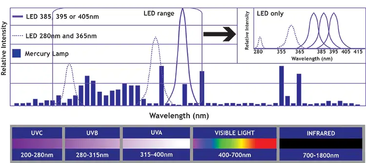
Advantages of UV LED curing include high spectral precision aligned with material photoinitiators; minimal infrared radiation and reduced substrate heating; stable spectral output over operating lifetime; and instant on/off operation without warmup.
These properties make narrow-wavelength UV well-suited for temperature-sensitive electronic components and assemblies.
Broad-Spectrum UV Sources
Broad-spectrum UV systems emit radiation across a wide wavelength range, including portions of UV-A and UV-B. These systems often are used with legacy UV-curable materials that rely on shorter wavelengths for activation.
Key characteristics described include:
- Compatibility with a wide range of UV chemistries
- Deeper penetration through pigmented or opaque materials
- Higher radiant heat output compared to narrow-band sources
Because of the increased heat and broader emission, additional shielding and cooling often are required when using broad-spectrum UV in electronics manufacturing.
Spectral Comparison
Across all UV curing approaches, technical guidance stresses the importance of monitoring irradiance and energy density at the cure site. Inadequate control can lead to incomplete curing, reduced adhesion or longterm reliability issues in electronic assemblies. Repeatability and output stability therefore are critical considerations in system selection and process validation.
UV curing plays a central role in electronics manufacturing by enabling fast, low-temperature curing of adhesives and coatings. Differences between spot and area curing systems determine whether precision or coverage is prioritized, while the choice between narrow-wavelength and broad-spectrum UV influences heat generation, material compatibility and process stability. By aligning curing architecture and spectral output with material and application requirements, manufacturers can achieve reliable, high-quality curing across a wide range of electronics processes.
 Stacy Hoge is a marketing manager at Excelitas, specializing in strategic messaging, brand positioning and customer-focused content development. She is responsible for the marketing communications strategy and implementation for the UV curing and photon detection product lines. Hoge is passionate about translating complex technologies into compelling narratives that drive engagement and growth. For more information, email Stacy.Hoge@excelitas.com or visit www.excelitas.com.