By Elisabeth Bodenstein and Uwe Vogel
Fraunhofer Institute for Organic Electronics, Electron Beam and Plasma Technology FEP, Dresden, Germany
Organic light-emitting diode (OLED) microdisplays are increasingly establishing themselves in consumer-ready wearables and data glasses. In order to meet the requirements for higher efficiency, higher contrast and higher resolutions in these applications, Fraunhofer FEP scientists have developed a new micropatterning approach for OLEDs on silicon substrates. This might eliminate the use of color filters and shadow masks in the future and allow full-color displays to be developed by means of a new process. An increase in efficiency and considerably broader color gamut already have been demonstrated in first experiments.
The average smartphone user looks at a display about 88 times a day, not counting viewing smaller smartwatches or other displays. Displays of all kinds have become ubiquitous and soon will be irreplaceable in everyday life.
The world of OLED microdisplays is immersed in data glasses for current and future virtual reality (VR) and augmented reality (AR) applications, the core of which is the microdisplay. Since the Pokémon Go mania, most individuals have an idea of what AR means – additional interactive information being interwoven into the real world. In addition to industrial use in Production 4.0 programs and products, its use in medical technology and in electronic entertainment, AR and VR applications also have been established for years in advertising and the education sector. The days of bulky audio guides in museums soon could be over – and not only as a result of previous solutions such as tablets and smartphones. Lightweight, head-up displays can turn exhibitions into expanded learning worlds by integrating film scenes, audio and visitor interaction to make a museum experience more memorable.

Thanks to the shallow overall depth resulting from the self-luminous properties of OLEDs and their excellent contrast ratios, manufacturers increasingly turn to OLED microdisplays for AR/VR glasses. Nevertheless, some technological challenges need to be mastered to exploit the full potential of OLED technology for use in consumer-ready data glasses and other AR/VR applications. Very high brightness and efficiency, good yields for large chip areas, curved surfaces, integrated eye tracking and transparent substrates are some of the tasks still on the researchers’ agendas.
To fabricate a full-color OLED display, red, green and blue (RGB) pixels have to be realized, which can be controlled separately. However, one remaining drawback in the current technology of OLED displays is the lack of options for micropatterning. Conventional photolithography is not suitable for organic layer patterning because the solvent process degrades the organic material. Hence, novel patterning techniques are needed to fabricate RGB OLED subpixels. Evaporation of organic material through fine metal masks is commonly used for OLED structuring, but the potential of this technique for higher resolutions is low. Another possibility is the application of color filters in combination with a white OLED, which has the advantage that the patterning of the semiconducting organic layers is not necessary. However, because of the filtering of the emitted light, this method results in low efficiency. Therefore, new concepts for OLED patterning are increasingly needed.

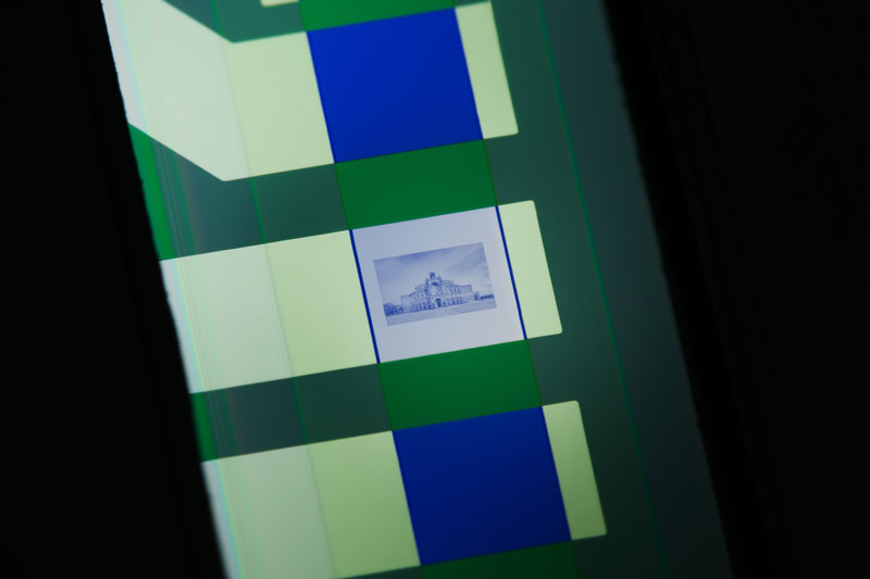
The use of electron beam technology for patterning applications in the field of organic electronics is an innovative approach. Two years ago, Fraunhofer FEP demonstrated the first results on electron beam micro-structuring of an OLED. There, the emission of a white OLED could be modified through an existing encapsulation layer. By applying a suitable acceleration voltage, the electrons can penetrate the encapsulation and interact with the subjacent organic layers. The localized electron absorption leads to degradation and chemical structure changes in the organic layers, which results in reduced luminance output of the OLED. To create high-resolution grayscale images in the OLED, the electron dose has to be varied pixel by pixel. An impressive example is the white OLED, in which the image of the famous Dresden Semperoper was written with the electron beam with a resolution of 12,700 dpi, which corresponds to 2 µm dot size (Figure 1). Using this patented technology offers the possibility to build the OLED highly productive and completely unpatterned before the emission is individually modified by the electron beam process.
Further development of the electron beam process has achieved full-color OLED without using color filters or shadow masks. The emission of RGB light for the different pixels is realized by microcavity-based mode selection from the spectrum of a white OLED. Microcavity OLEDs are commonly known and have been investigated extensively. Basically, the microcavity OLED consists of an organic layer stack sandwiched between two metal electrodes. One electrode constitutes the reflective metal mirror on one side; the other one the semitransparent metal mirror on the opposite side. Together they build the resonator. The layer thickness of the complete stack defines the resonator length. By varying the organic layer thickness between the two electrodes, it is possible to adjust the resonant wavelength of the cavity and obtain RGB emission from a white top-emitting OLED.
A thermal electron beam process is used for the realization of the different layer thicknesses. After the deposition of the first organic layer, material is ablated locally by electron beam processing. The process continues with another deposition of organic material, a second patterning step and another deposition, which results in a staircase of three different layer thicknesses on the respective pixels for RGB. The OLED stack is finalized by on-top evaporation of additional layers. Finally, the metal electrodes form a staircase of microcavities that enable RGB colors according to the different resonator lengths.
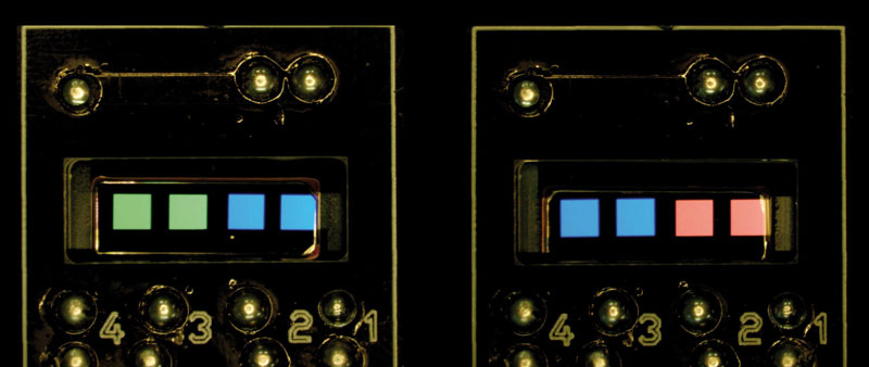
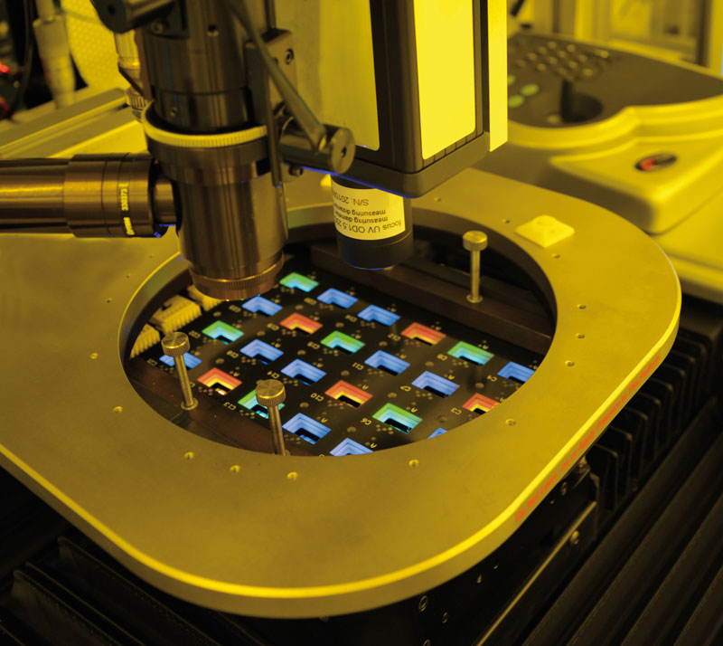
The feasibility of this approach could be successfully demonstrated by established simulations and a following proof of concept. RGB emission was demonstrated on first test substrates, exhibiting comparable OLED performance (Figures 2 and 3).
In addition to using this new process for OLEDs, electron beam processing also can be used for other applications in organic electronics and inorganic layers. Moreover, the electron-beam patterning process is very adaptable and can be employed in the areas of photovoltaics, microelectromechanical systems (MEMS) and thin-film technology.
Now scientists are approaching the next milestones, having completed the promising preparatory work. The main goal in the coming years is to use this new method in jointly developing fabrication of OLED microdisplays with partners and establish the process in the industry through licensing. To do this, the features will be further miniaturized and the process optimized by working together with interested partners from industry. The next step planned is to integrate the micropatterning into existing processes to gain further know-how jointly with industrial partners. This should enable future transfer of the test results into an existing process line to facilitate establishing the technology at the industrial level.

In parallel, scientists also plan an enhanced simulation of OLEDs. The OLED color spectrum will be broadened by suitably modifying the materials and layer thicknesses. In this way, the prospective incorporation of the displays in data glasses for special applications – such as in industrial manufacturing and medicine – should be opened to the new process.
The Fraunhofer Institute for Organic Electronics, Electron Beam and Plasma Technology FEP works on solutions in the fields of vacuum coating and surface treatment as well as organic semiconductors, offering possibilities for research, development and pilot production, especially for the processing, sterilization, structuring and refining of surfaces, as well as OLED microdisplays, organic and inorganic sensors, optical filters and flexible OLED lighting.
Elisabeth Bodenstein is research associate at the Fraunhofer Institute for Organic Electronics, Electron Beam and Plasma Technology FEP in Dresden. She is responsible for electron beam micropatterning, surface modification and related applications. Her research fields include various patterning technologies, semiconductor and display technologies, and OLED topics. She can be reached at Elisabeth.Bodenstein@fep.fraunhofer.de.
Uwe Vogel started as a skilled worker in semiconductor microelectronics in 1983, before he earned his diploma in information technology in 1991 and his doctoral degree in biomedical engineering in 1999. Since 2010, he has served as the head of division “Microdisplays and Sensors” and since 2014, Deputy Director of Fraunhofer FEP. He can be reached at Uwe.Vogel@fep.fraunhofer.de.


