Any discussion of 3D processing these days almost immediately turns to additive manufacturing – in which electron beam does indeed have a role1,2 – but outside the scope of 3D printing lie plenty of challenges for UV and EB in this 3D world. In contrast to thermal processing, users of UV/EB must be cognizant of how a curve or an angle or any similar complexity will affect the energy distribution over a 3D surface. This is one of the primary reasons why traditionally low-energy, area-type3 electron beam (≤ 300 kV) has been a processing technique for flat, roll-to-roll web applications, such as cross-linking plastic films or curing overprint varnish on printed substrate. Most current industrial electron beam installations are configured to process web-based product. However, electron beam does not have to be relegated to 2D applications; customer need, advancements in the technology and a bit of ingenuity have caused a movement of EB into the third dimension.
Yet, there can be challenges in using EB to process complex geometries. First and foremost is the challenge of shielding. Accelerated electrons produce bremsstrahlung x-rays when interacting with matter.4 The electron beam system must be shielded – often with lead – to contain these x-rays and provide a safe working environment. Designing shielding to accommodate the movement of 3D products into and out of the beam requires more skill and ingenuity than that needed for a thin film. In addition, the vacuum system that accompanies the beam (the electrons must be produced and accelerated in high vacuum) can be cumbersome to creative configurations. This challenge has been greatly alleviated by the advent of sealed EB emitters, in which the required vacuum is achieved during production of the emitter, the emitter is sealed and no vacuum equipment is necessary for operation.5 The lack of vacuum equipment makes the sealed emitter more compact and nimble than a traditional EB system.
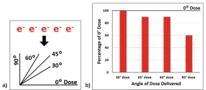
Despite these challenges, there are multiple ways that electron beam can be used to process 3D products. The first way is to simply be aware and make use of the electron scatter. The accelerated electrons the beam produces don’t just interact with the product in an orderly, unidirectional manner. Instead, they are scattered every which way as they collide with the window foil and then air molecules before reaching the product. Accelerating voltage is an important aspect of the electron scatter, and higher voltages (i.e., ~150 to 300 kV) may be required to overcome the larger distances between the beam and the product than are experienced with flat substrates. Radiochromic dosimeters can be used to quantify the energy distribution over complex geometries. Figure 1 shows an example of using dosimetry to determine the dose distribution at multiple angles. These results indicate that, at 200 kV, even a surface orthogonal to the beam (90°) receives 60% of the dose that was seen by a flat surface (0°). While electron scatter alone will not reach 360° around a product, it can be used for non-flat products, such as those with curved surfaces.
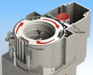
If electron scatter isn’t sufficient, another way to achieve energy distribution in 3D is to articulate the product, presenting every side to the beam. A classic example of this is the process of festooning cables to cross-link the cable insulation.6 The cable is run back and forth under the beam multiple times, and at each pass it is turned so that once it has exited the beam, every angle has received an equal dose. Another possibility is to spin the product as it is passed once in front of the beam, again exposing every angle equally. An example of this type of configuration is shown in Figure 2: The drum rotates the cylindrical parts in front of the EB emitter, and, simultaneously, the parts are spun for complete exposure.
Depending on the product, it may be preferable to articulate the beam emitter instead. A sealed emitter makes it feasible to angle the beam in one direction, then, for example, change that angle before the product is presented to the beam a second time. Attach a sealed emitter to a robotic arm and just about any angle is achievable.
Finally, 3D electron beam processing also can be accomplished with multiple emitters. Two emitters, both facing inward, can be used to irradiate both the top and bottom of the product as it passes between them. This method can be combined with articulation of the product by causing it to freefall as it passes through both beams.7
When choosing EB to process complex geometries, it is good practice to consider the different configuration options. Some options may be more feasible or cost effective than others depending on the handling of the product, complexity of design, amount of shielding necessary, number of emitters, etc. Whatever the case, know that EB in 3D is a possibility!
 Sage Schissel, Ph.D.
Applications Specialist
PCT Ebeam and Integration LLC
sage.schissel@pctebi.com
References:
- Gonzales-Martinez, I.G., Bachmatiuk, A., Bezugly, V., Kunstmann, J., Gemming, T., Liu, Z., Cuniberti, G., Rummeli, M.H., Electron-beam induced synthesis of nanostrucutures: a review. Nanoscale, 2016, 8, 11340-11362.
- Kumar, S., Additive Manufacturing Processes. Springer International Publishing, 2020.
- Mehnert, R., Pincus, A., Janorsky, I., Stowe, R., Berejka, A., UV & EB Curing Technology & Equipment. John Wiley & Sons, Inc.: London, 1998.
- Chapiro, A., Radiation Chemistry of Polymeric Systems. John Wiley & Sons, Inc.: New York, 1962.
- Haag, Werner, Sealed electron beam emitter for use in narrow web curing, sterilisation and laboratory applications. RadTech Conference Proceedings 2012.
- Makuuchi, K., Cheng, S., 2012. Radiation processing of polymer materials and its industrial applications. Wiley.
- Laatu: Non-thermal, in-plant microbial reduction solution for dry foods. Buhler, 2019. https://www.buhlergroup.com/content/buhlergroup/global/en/services/Digital-services/laatu.html