The first seven editions of “Professor’s Corner” focused on the fundamentals of polymer chemistry as they apply to the field of UV/EB polymerization. In this eighth edition, a special topic is introduced. It is probably not well known that a typical UV/EB polymerization process produces films that contain vast numbers of particles or domains or phases known as “microgels.” This article introduces this mysterious species that is lurking in most all energy-cured films, particularly those based on (meth)acrylate-functional monomers and oligomers and produced by free radical addition polymerization processes.
What is a microgel? In photopolymerization, microgels are amorphous cross-linked particles that range from roughly 50 to 100 nm in size.1 They are imbedded in the cross-linked polymer matrix and represent a separate phase from the network, which itself is typically amorphous! Not only are they of varying size and shape, they also possess very different morphologies from each other and from that of the network polymer matrix. Each microgel domain, in principle, will exhibit its own particular glass transition temperature (Tg). Recall that the Tg is a property of amorphous portions of a polymer film only.
One might rightly ask why such photopolymer films are transparent rather than hazy or cloudy, as with other multiphase heterogenous mixtures, such as colloids. The transparency is a strong indication that, in such cases, it is probably inappropriate to label them as “microgels.” Rather, they are “nanogels.” Were they actually of micrometer (mm) size, such a multiphase system would scatter visible light, producing translucent or opaque polymer films.
Microgels are well-known entities, often of mm size, that are typically introduced intentionally into various polymer matrices to provide a variety of property enhancements. But these applications are not being considered in this discussion of photopolymer nanogels.
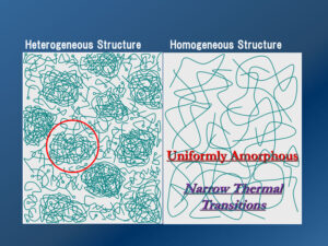
Heraeus Japan.
Who cares? Tens of thousands of perfectly fine UV/EB-polymerized coatings, inks, adhesives and other end-use products are produced every day that are not negatively impacted by the presence of nanogels. So why do they matter? There are at least three answers to this very valid question: 1) In many, if not in most applications, they don’t matter! 2) There is value in knowledge for its own sake. The more we understand about the fundamental nature of the UV/EB polymerization process and the molecular structure of the products produced by this technology, the more well prepared we are to interpret experimental results and to address problems when they arise. 3) Since the nanogels represent separate phases, the interface between them and the polymer matrix represents locations where stress can build up and cracks can propagate, causing enhanced brittleness. So, in applications where impact resistance is needed, for example, the nanogels might lead to application failure.
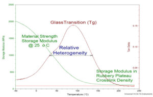
Grasping the concept. Figure 1 provides a conceptual image of a UV/EB polymer matrix with embedded nanogels.2 The right side of the figure shows a uniformly amorphous structure. Of course, the word “amorphous” literally means “without structure.” We can think of this as being “homogeneously heterogeneous.” In contrast to this image, the left side of the figure shows a polymer matrix with imbedded nanogels of varying sizes and shapes. This represents heterogeneity at the molecular level. This morphology will produce a wide Tg temperature range, since each nanogel and the matrix itself may, in principle, all have different Tgs. In a dynamic mechanical analysis (DMA) scan, this will be indicated by a quite wide half-height width of the tan d curve. In Figure 2, the half-height width is roughly 100°C! Also, it has a “shoulder,” indicating a tendency, in this particular case, toward a bimodule distribution of nanogels in the film. Recall the discussion of the tan d curve in a previous edition of “Professor’s Corner.”3 This curve represents a range of different Tgs within the polymer sample. The peak of the curve represents the Tg of the largest cohort of similar amorphous domains and is typically reported as the Tg of the sample. Were there no nanogels present, the tan d curve would be much narrower. In the ideal limit of a perfectly uniformly amorphous morphology, it would be a “spike.”
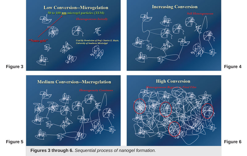
Figures 3 through 6 depict schematically the sequential process of nanogel formation during a UV polymerization process. These are images graciously provided for use in presentations by the late Charles E. Hoyle of the University of Southern Mississippi. In Figure 3, there is very little conversion to polymer, and the nanogels are beginning to form. In Figures 4 and 5, the nanogels continue to increase in concentration. Finally, in Figure 6, the full polymer network has formed, demonstrating a complex amorphous structure with a high concentration of nanogels at the end of the process.
What causes nanogels to form? Nanogels form primarily through a process described as “cyclization.” This process causes entrapment of free radicals, reducing the overall conversion of multifunctional monomers and oligomers to polymer and, at the same time, producing nanogels. The discussion of the formation of nanogels will be continued in a future edition of “Professor’s Corner.”
Technical Questions?
What are your technical questions about polymer science, photopolymerization or other topics concerning the chemistry and technology of UV/EB polymerization? Your questions will help guide future topic decisions for this column. Please submit your questions via email to Dianna Brodine at dianna@petersonpublications.com.
 Byron K. Christmas, Ph.D.
Professor of Chemistry, Emeritus
University of Houston-Downtown
b4christmas@gmail.com
References
- Hoyle, Charles E., personal communication, 2008.
- Image produced by Fusion UV Systems Japan KK (now Heraeus Japan) in 2008 and used by permission for presentation at RadTech Conferences, Heraeus Japan UV Seminars, and this column.
- Christmas, B. K., “Professor’s Corner,” UV+EB Technology, 6, No. 2, 2nd Quarter, 2020, pp. 12-13.


