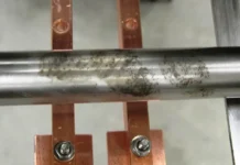
In the preceding column, I compared the feature size and print area of the principal UV vat printing technologies from large to small and their relevance to commercial applications. 1 This column reviews current and future applications of the additive manufacturing of ceramic materials as critical components in electronic devices, an industry in which small feature size is fundamental.
Ceramics

Ceramics are of great interest in electronics applications for many reasons. Typically composed of Aluminum Nitride, Silicon Carbide, Alumina or Zirconia, they provide mechanical strength, chemical and wear resistance, low thermal conductivity due to their porous structure, low electrical conductivity and coefficients of thermal expansion (CTE) comparable to silicon and other materials used in device construction. 2 The CTE is critical to ensure that the integrity of electrical connections is maintained during the thermal cycling of power, logic and memory devices. The last two properties, low electrical conductivity and low thermal coefficients of thermal expansion, are desirable for electronics applications, as current leakage and substrate warpage are significant failure modes. The mechanical properties that make ceramic materials useful also make them difficult to machine, particularly for components with small dimensions and complex geometries. For this reason, Vat polymerization has become an important method for overcoming the design limitations of subtractive manufacturing. As the parts still require sintering to volatilize organics and fuse together, the fundamental property advantages of ceramic materials are not compromised. 3
Digital Light Processing (DLP) vat polymerization of ceramics recently has been applied to the construction of a compact quantum frequency reference device (shown in Figure 1) using printer technology commercialized by Lithoz to construct a micro-optical bench from Alumina that normally would occupy a tabletop. 4 Frequency references are important for earth- and space-based navigation and timekeeping, and stability against the effects of thermal, mechanical and radiation exposure is critical to their operation.
In an interesting modification of a normally insulative material, Zhou and colleagues incorporated graphene into a silicon carbide ceramic structure to obtain a material with low density and high electrical conductivity, as well as low thermal conductivity and temperature stability up to 600° C. The ceramic graphene composite presents a distinct advantage in comparison to metals, which have high thermal conductivity and a strong dependence of electrical resistivity on temperature. In addition, the conductivity of the composite can be tuned by adjusting the concentration of graphene in the matrix. 5 The properties of the composite and its incorporation into an electrical circuit are shown in Figure 2.

In order to incorporate increasing numbers of chiplet components into a device, designers increasingly are relying on expansion in the vertical direction in order to increase complexity without increasing area. Increasing the length of interconnects reduces the circuit speed, which is counterproductive for memory-processor data transfer. In order to integrate semiconductors into a device, electrical traces, called vias, are required to bridge devices in a manner that is mechanically stable over a wide range of conditions. This function is fulfilled by an interposer, a dielectric material that prevents the electrical traces from interacting with each other through interchannel crosstalk. The interposer typically is glass, ceramic or silicon as shown in Figure 3. 6

As the dimensionality of devices decreases, the spatial density of these channels increases, and with it, the desirability of being able to route channels in three dimensions rather than simply in straight lines. Using an amorphous silica nanopowder incorporated into a UV-curable siloxane, a team from HRL Laboratories has used printer technology from Boston Micro Fabrication to print an interposer for a nonplanar imaging sensor, resulting in a high pixel density and feature dimensions as small as 10 microns. As illustrated in Figure 4, the vias formed in the ceramic interposer were filled with a molten conductive alloy and integrated with an infrared detector and readout integrated circuit (ROIC), which collects and processes the detector signal. 7

Additional topics in additive manufacturing, such as volumetric 3D printing, sustainability and biomedical applications, will be discussed in future columns.
References
- This column is focused on photopolymer applications in additive manufacturing in which a reservoir or vat of liquid resin is photopolymerized layer by layer to generate a part. When a layer is cured using a narrow laser beam in a series manner, one point at a time, it is referred to as stereolithography or SLA. Simultaneous illumination of a large area to cure one full layer at a time can be accomplished with a digital light projector (DLP) or a liquid crystal display (LCD) screen. There also are many permutations of these approaches which may utilize multiple light sources and optics to achieve specific performance advantages.
- https://ceramics.org/about/what-are-ceramics/structure-and-properties-of-ceramics/ (accessed March 7, 2025)
- Lin, H.; Shen, Q.; Ma, M.; Ji, R.; Guo, H.; Qi, H.; Xing, W.; Tang, H. 3D Printing of Porous Ceramics for Enhanced Thermal Insulation Properties Advanced Science 2025, 12, 2412554-2412573
- Christ, M.; Zimmerman, C.; Neinert, S.; Leykauf, B.; Doeringshoff, K.; Krutzik, M. Additively Manufactured Ceramics for Compact Quantum Technologies Advanced Quantum Technologies, 2024, 7, 2400076-2400084
- Guo, Z.; An, L.; Khuje, S.; Chivate, A.; Li, J.; Wu, Y.; Hu, Y.; Armstrong, J.; Ren, S.; Zhou, C. 3D-printed Electrically Conductive Silicon Carbide Additive Manufacturing 2022, 59, 103109-103115
- Li, Y.; Goyal, D. 3D Microelectronic Packaging: From Architectures to Applications Springer 2021
- Schaedler, T.; Porter, K.; Yu, A.; Soukiazian, S.; Sasse, T.; Wernick, E.; Bui, P.; Hundley, J.; O’Masta, M. Additive Manufacturing of Interposers with Curved Vias for Microelectronics Packaging Additive Manufacturing, 2025, 98, 104642-104651


