


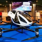
By Michael Bonner, vice president of engineering & technology, St. Clair Systems According to the National Business Aviation Association (NBAA), “AAM is a new concept of air transportation using electric vertical takeoff and landing (eVTOL) aircraft to move people and cargo between places not currently or easily served by surface transportation or existing aviation modes. … [Read more...] about Opportunities for Energy-Cure Coatings in the Advanced Air Mobility Marketplace
Articles
Regulatory News – 2026 Quarter 2

EPA Loosens Rules, Limits States’ Authority The Environmental Protection Agency (EPA) recently has made various decisions that reverse some state and local air district regulations and diminish their regulatory authority. EPA Repeals Endangerment Finding In 2009, the EPA issued the Endangerment and Cause or Contribute Findings for Greenhouse Gases under the Clean Air Act … [Read more...] about Regulatory News – 2026 Quarter 2
Count Everything: What Gets Measured, Gets Improved
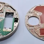
In the 1999 baseball movie, For Love of the Game, there is an exchange between Kevin Costner (Billy) and Kelly Preston (Jane): Jane: Do you lose very much? Billy: I lose. I’ve lost 134 times. Jane: You count them? Billy: We count everything. In UV, we also need to count or measure everything because, as Lord Kelvin said, “If you cannot measure it, you … [Read more...] about Count Everything: What Gets Measured, Gets Improved
EB and UV for Coil Coating: Solutions, Challenges and Managing the Transition, Part 3
Editor’s Note: Part 1, which appeared in Quarter 3 UV+EB Technology, discussed how EB and UV were practical and sustainable solutions for the coil coating industry. Part 2, which appeared in Quarter 4 UV+EB Technology, hosted a discussion on the value of savings related to the reduction in energy consumption and other factors, as well as the reduction in safety hazards for the … [Read more...] about EB and UV for Coil Coating: Solutions, Challenges and Managing the Transition, Part 3
Volumetric Additive Manufacturing

The UV additive manufacturing techniques discussed in this column have focused on approaches in which the part is printed layer by layer in series. 1 The current column reviews technical approaches to volumetric additive manufacturing (VAM, also referred to as Deep Vat Printing, or DVP), a general class of additive techniques in which the part is freely suspended within the … [Read more...] about Volumetric Additive Manufacturing