By Liz Stevens, contributing editor, UV+EB Technology
Researcher Janos Veres and his colleagues at the Palo Alto Research Center (PARC) are shaping the future with their research and development – and with a helping hand from UV technology. Across projects as diverse as a “smart” mouth guard for athletes, a printed and embedded circuit with its own NFC antenna, and a multi-technique printer that combines three printing technologies and two curing methods, UV technology can be found playing a part in many of the innovations in Veres’ portfolio.
The Palo Alto Research Center, located in Palo Alto, California, is a subsidiary of Xerox Corporation, initially founded in 1970 and established as an independent company in 2002. The center has six main foci:
- AI and human-machine collaboration
- Digital workplace
- Novel printing
- IoT and machine intelligence
- Digital design and manufacturing
- Microsystems and smart devices
At PARC, 175 researchers from 22 countries provide R&D and other services for clients ranging from Fortune 500 and Global 1000 firms to government agencies and start-ups worldwide. The researchers’ work has led to more than 2,000 patents, 4,000 scientific papers and 100 books.
Veres is program manager, Printed and Novel Electronics at PARC. His research revolves around creating electronics in new form factors, including large, flexible and conformal image sensors and detector arrays; exploring flexible, hybrid printed electronics for use in customized IoT devices; employing smart inks that can add electronic functionality to automotive and wearable devices; and investigating microchip inks from which electronics can be created and instructed to configure themselves, change shape or even disintegrate.
Of PARC’s six areas of focus, Veres concentrates on two: Microsystems and Smart Devices, and Novel Printing. His passion for pushing the envelope is contagious, and so is his enthusiasm for the possibilities – probabilities – for flexible, conformable electronics, seamlessly integrated electronics and the on-demand manufacture of electronics.
Veres summarized the nature of his recent research. “For the last two years or so, we’ve been working on leveraging the printing know-how that already exists with the innovation that exists at PARC,” he said. He hopes to see how the combined expertise can be deployed in the electronics industry. Veres anticipates the development of new printing techniques that use novel materials to build electronics “with new form factors that are flexible, accessible and foldable, and that may be thermoformable.”
His goal is not to create things by squeezing electronics into a particular shape – which is typically how people view microelectronics – but, rather, to create what could be called macroelectronics, “relevant for things that interface with the world and with people, like automotive interiors, wearable devices or sensors on aircraft wings.” The macroelectronics that Veres envisions, he said, “will require new form factors, often new materials, and new deposition techniques.”
Veres described the environment at PARC in vivid terms. “What we are doing at PARC is that we are operating, let’s say, a time machine,” he said. “We are thinking ahead – what could the world look like if we had these technologies at our fingertips? That’s why we experiment and develop things that could change electronics manufacturing.”
Veres’ experiments and development projects are difficult to categorize as strictly a quest for this cutting-edge device or that novel process. For Veres, R&D on new devices can lead to the creation of fresh problem-solving processes, and exploration of emerging processes can open doors for imagining new functional devices.
In some cases, Veres explores existing but relatively new technology, such as 3D printing, and uses it as a jumping off point. “Most of 3D printing is directed to creating structures,” he said, “shapes that are difficult to obtain with conventional techniques.” Veres pushes the envelope, to take 3D printing to a new incarnation. “What we envision is that there will be a need to make these things smart, to actually add functionality to them so that they carry current or so that they send signals.”
In other cases, Veres seems to be reimagining a process altogether, as with his work in developing a smart label with printed sensors, a printed antenna and bare die chips. Veres also described a futuristic UV-cured embedded circuit. “It’s an NFC antenna,” he explained, “and this is built up as a monolithic piece from a UV-curable dielectric with the silver printed in the middle of the structure.”
In product creation, designers often must make a choice as to what takes precedence – form or function. For Veres, the choice apparently is an emphatic “Both!” His impetus to design and refine flexible, conformable electronics results in high functionality that is molded (literally) into the desired form.
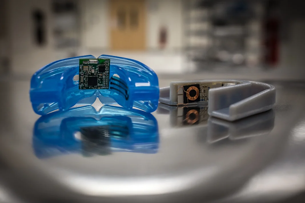
One such device that Veres is refining is a wearable device – a three-dimensional, customizable lactate biosensor in a mouth guard. Envisioned for athletes to help monitor their performance and now in the piloting stage, this sensor is built into a mouth guard structure that initially is UV-cured.
The electronics for the biosensor feature enzyme-based printed biosensors, flexible and conformable circuitry, communications to send the sensed lactate levels to a smart watch via Bluetooth Low Energy and a wirelessly rechargeable battery. After the integration of its technology, the mouth guard structure can be thermoformed to the shape of an individual’s mouth.
Another device that Veres is refining is both device and process. It is an integrated printing platform that includes a multi-technique printer along with multiple curing technologies. Arrayed in one platform are heads for inkjet, aerosol jet and extrusion printing, a heated platen for thermal curing, and blocks for UV and radiant thermal curing. Engineers and software experts at PARC collaborated to develop this platform, which also included developing the workflow for driving the printers. In addition to controlling the printing and curing via software, the platform allows for computerized control of XYZ motion, and for droplet and surface visualization.
Veres notes that prototyping printers do exist on the market, but not in anything like the configuration that PARC has produced. “There are prototyping printers out there which you can buy from various equipment manufacturers that, say, give you an inkjet platform or an extrusion platform,” he said. “Or they separately sell you flash cure equipment or high-intensity photonic curing or aerosol jet. What we are doing is combining them because then we can do sequential printing of different materials.”
The platform’s UV curing block is of great benefit. “As we print inkjet dielectric, we can UV cure them right away,” Veres explained, noting that UV curing instantly produces the required solidified interior for dielectric.
The integrated platform offers additional benefits. “Another reason why you need the different types of techniques is that you want to bring together different material systems,” said Veres, “and they will have different viscosities.” Some structural materials that may be utilized include urethanes, silicones, epoxies, acrylics, phase changes and hydrogels. Particle-based and precursor conductive materials also are common in the type of printing envisioned for Veres’ platform.
The inkjet, spray and extrusion printing methods bundled into the platform are compatible with their own range of viscosities. “Aerosol jet actually is a very unique technique,” said Veres, because it spans the viscosities of ink jet and extrusion printing. This technique is still being fine-tuned. “It’s very powerful,” he said, “but it’s typically a single nozzle technique and we don’t know yet how it is going to scale.”
The PARC integrated printing platform is configured, as of now, for printing sheets. “But it does have the ability to move on to rolls,” said Veres. “Ultimately, when we truly understand the need for high-volume manufacturing, we can transition it to rolls, but we probably won’t be stopping there.”
While UV curing technology is only a part of Veres’ arsenal of techniques for fabricating the future, he points out some unique and important benefits of using it. “We use UV curing, in particular,” explained Veres, “for dielectric and structural materials for electronics, in a very similar way that UV curing is used for 3D printing and with inkjet-based curing.”
In his work on printed electronics, Veres seeks to replace the many discrete components that typically are assembled and affixed to a circuit board. “Quite a few of them can be readily transitioned to printable versions,” he said, “and that means electronics boards that you now see with discrete resistors can instead use printed resistors which become seamless with the board itself.” Seamless printing and integration of components, however, poses problems. “There is an important challenge in printing electronics that is actually very similar to printing on nonporous surfaces in the conventional printing industry. Because when it comes to printing on plastic, the surfaces are non-absorbing.
“You want to print fast and so there must be some technique to solidify the ink as it coats the product,” he continued, noting that the packaging industry already has solved this dilemma by using UV-curable inks. “We can deploy similar techniques for UV curing when it comes to printing dielectric layers,” he explained, “and that is very useful.”
Veres went on to describe another option for photonically curing nonoparticle metals (silver or copper) as part of the process of printing electronics. “The traces that are required for these electronics, very often they are photonically cured, and people use Xenon flash which is mostly visible light,” he said. “It might have on the tail end a little bit of UV, but the benefit is that you provide the energy to melt nanoparticle metals very rapidly. The metal particles in the inks are made from 10- to 15-millimeter size metal nanoparticles. When the particles are tiny, their melting temperature is much lower, so if you present a very high-intensity flash, you almost instantly can melt the particles without melting the plastic substrate underneath.
In a comment to the consortium of UV curing scientists and professionals, Veres offered this: “If there is one message for the UV curing community, it is this: There is this interesting area of printing electronics where UV-curable material can give a benefit because it allows for immediately solidifying the dielectrics that are not in between traces in the X and Y dimensions.”
At PARC, the future looks bright thanks to the hard work and fertile imagination of researchers like Janos Veres – and with a little help from UV.


