


By Neal T. Pfeiffenberger, Ph.D., Sartomer Americas
UV-curable electronic materials require a unique set of expertise in resin formulation, processing and end-use properties. Commercial uses for UV-curable electronic products include conformal coatings, potting, photoresists, display materials and adhesives, as well as various 3D printing applications. This paper will focus on using dielectric testing techniques to quantify a wide range of electronics resins for these growing applications.
Introduction
Dielectric performance is highly important for a variety of electronic applications. It controls how the material reacts under electric field and/or a change in frequency. Temperature, humidity, mechanical forces, surface structure, defects and porosity can affect the resultant dielectric properties.
Capacitor film has been an area of interest for UV-curable materials due to its self-healing properties. Much work has been performed in this area around the development of high-temperature thermoplastic films, which are capable of functioning as a DC-link capacitor for hybrid electric vehicles featuring wide band gap semiconductors,,. Acrylate-based self-healing layers are known in the capacitor film space but are limited by high-temperature performance and typically are highly polar,. New materials are being evaluated in this space based on dielectric performance vs. frequency as well as high breakdown strength.
Ultra low loss materials for dielectric coatings are another application area of interest for UV-curable materials. These materials can be used as dielectric layers to minimize their effect as a substrate when exposed to changing frequencies or high electric fields. Most commonly, they are used as insulating layers for multi-layer circuits.
Damping materials are widely sought after for sound and vibration elimination for a variety of applications. Damping materials related to electronics include optical camera image stabilization modules, microphones and speakers, shock absorption, displays, robotics and motor/compressor noise. Silicone-based UV-curable materials are optimal for these applications, but a recent focus on insulating acrylate-based material systems will be considered.
UV-curable potting materials are useful in applications that require shallow depth of cure (typically up to 0.25 inches), have temperature-sensitive components and need a fast, in-line production process. They also feature nearly unlimited working times compared to conventionally thermally cured systems if kept in a dark environment. UV-curable potting materials typically make a rigid bond with excellent adhesion to plastics with good chemical resistance and excellent insulation properties.
Most of the above applications are typically thermal cured using conventional peroxide curing agents. UV curing presents alternative means of processing, which can allow for thermally sensitive electronics, faster processing times and comparative dielectric properties.
Experimental Setup
Film samples were cured with a broadband Dymax flood lamp (5000-EC) at 250 µm thick on both sides to ensure a full cure. The samples were conditioned prior to testing by heating to approximately 25ºC below the material’s glass transition (Tg) temperature to remove any absorbed moisture. Cured film thickness was measured using a Heidenhain Metro gauge accurate to ± 0.2 µm. Three locations in a 1.0 cm2 area were chosen for film thickness measurements prior to screen printing of conductive ink, and their average was used for the dielectric constant and volume resistivity calculations.
Breakdown strength of cured films was measured using the ASTM D-149 standard, ramping at 500 V/s. This test utilizes a 6.35 mm stainless steel ball on a brass substrate in 25ºC silicone oil to minimize the electric field non-uniformity and the chances of a film defect being present at the test location. The cured film thickness was measured and recorded in each breakdown location prior to breakdown. Twenty measurements were made on each film, and the dataset was fit using a 2-parameter Weibull distribution with a 95% confidence interval.
Dielectric Constant and Loss was measured using an LCR meter at room temperature via the ASTM D-150 standard. One side electrode of the capacitor was connected to a high-voltage and high-current terminal of an LCR meter and the other electrode of the capacitor was connected to a low-voltage and low-current terminal. A 2 VAC bias was applied to each sample during the measurement.
Surface and Volume Resistivity was measured using a Keithley 6517B and 8009 fixture at room temperature via the ASTM D-257 standard. An alternating polarity of ±100 V was applied to the cured film for 10 seconds with a 2nA current range prior to measurement to ensure a net zero charge.
Results and Discussion
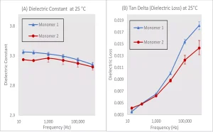
Two monomers have been analyzed specifically for use in the capacitor film coating application. Monomer 1 is a conventional off-the-shelf material with good thermal and mechanical performance from -40 to 150°C. Monomer 2 is an optimization of Monomer 1 that statistically decreases the dielectric loss at higher frequencies and only slightly decreases the dielectric constant of the material over the 20Hz to 1MHz operation range. As SiC MOSFETs and IGBTs become more prevalent on the market due to a decrease of on-state resistance, their wide band-gap performance has necessitated a higher operational temperature and frequency. Understanding how to modify the chemistry of the monomers to decrease the dielectric loss of the materials at high frequency is of utmost importance for optimal material down selection. Figure 1 (A) shows Monomer 1 and 2 having the same trend in dielectric constant vs. frequency as measured with the LCR meter. Figure 1 (B) outlines a similar performance at low frequencies, with a statistical difference present above 1kHz.
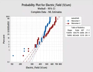
Breakdown strength of Monomer 1 and 2 were measured using the ASTM D-149 standard as described in the Experimental section above. Figure 2 shows the results of the 2-parameter Weibull analysis at 25ºC. A statistical difference in dielectric breakdown strength can be seen, with Monomer 2 having approximately 100V/µm greater dielectric strength.
Optimization of dielectric loss is a key factor in many applications like dielectric substrates, device encapsulation, thermoset film capacitors and potting materials. New hydrophobic resin blends have been developed to optimize the low loss needs of these applications while still maintaining good breakdown strength characteristics. Humidity strongly affects the dielectric materials that are hydrophilic and can increase capacitance and loss significantly at 85% relative humidity. When fillers are added to the matrix to increase dielectric constant and not change dielectric loss without functionalization of the particles, detrimental effects typically occur by a drastic reduction in the shape and scale parameters of the Weibull breakdown results. Figure 3 shows three new resin blends that have been developed that significantly reduce the dielectric loss of the material while keeping the dielectric constant stable vs. frequency.
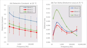
All three resin blends show differences in dielectric constant and loss over the 20 Hz to 1 MHz range. Blend 1 has the highest dielectric constant, with a good average dielectric loss over the range of frequencies. A high dielectric constant is preferred in most applications, as this can increase the capacitance for the same film thickness. Blend 2 shows the lowest dielectric constant vs. frequency and lowest dielectric loss up to 100 kHz before trending higher. Blend 3 shows a dielectric constant of 2.65 to 2.8, with very low loss at 1 MHz that is continuing to trend lower. For higher frequency applications, this would be the preferred blend based on its dielectric performance.
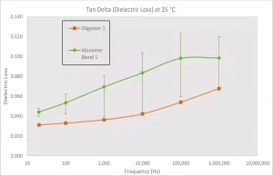
Damping behavior is governed by the orientational polarization of the material (called the dipole moment). Materials with a high dipole moment are well correlated with their respective mechanical loss factors and shear compliance values. Oligomer 1 and Monomer Blend 1 shown in Figure 4 are good examples of acrylate-based polar resins that have high dielectric loss and excellent damping behavior over a wide range of frequencies. As seen in Figure 4, Monomer Blend 1 has a larger variation due to the limited adhesion of the screen printed conductive ink in all of the samples. Oligomer 1 is a much harder material compared to Monomer Blend 1, which allows for better adhesion of the conductive ink.
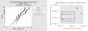
Ultra-hydrophobic UV potting resins have been developed to work at a wide range of temperatures, have high volume resistivity and high breakdown strength, while maintaining good thermal and mechanical shock resistance. In certain applications, a thermally cured potting solution could damage temperature-sensitive electronic components. Figure 5 (A) shows the room temperature breakdown strength of Resin Blend 1 and 2, with a target viscosity of 5 kcPs for easy application in a manufacturing environment. High breakdown strength values of 580 to 654 V/µm with high shape factors indicate great dielectric strength and high repeatability. Figure 5 (B) shows the relationship between surface and volume resistivity, which are important factors in determining how good of an insulator the respective blends are as a function of voltage. The higher the values of surface and volume resistivity, the better the insulator is at isolating voltage under electric field.
Conclusion
Herein we have identified next-generation materials that are capable of being optimized for each respective application. Cured resins have been showcased for examples in capacitor film coatings, low loss dielectrics, audio/vibration damping and UV-curable potting materials. The common themes of these materials include the need for high breakdown strength, low moisture uptake, very low or very high dielectric constant and high resistivity values. These examples of new materials show how electronic properties can be optimized specific for an application by optimizing the chemistry of the resin. υ
The materials mentioned in this article are commercially available through Sartomer by request but typically are tuned for the specific substrate or application of interest. For more information, visit https://americas.sartomer.com/en/.
References
- N. Pfeiffenberger et al., “High temperature dielectric polyetherimide film development,” IEEE Trans. Dielect. Electr. Insul., vol. 25, no. 1, pp. 120–126, 2018.
- Zhang, X.M., Liu, J.G., Yang, S.Y.: ‘A review on recent progress of R&D for high-temperature resistant polymer dielectrics and their applications in electrical and electronic insulation,’ Rev. Adv. Mater. Sci., 2016, 46, (1), pp. 22–38
- Fan, Baoyan et al. “Dielectric materials for high-temperature capacitors.” (2018).
- A. Yializis. “A Disruptive DC-Link Capacitor Technology for Use in Electric Drive Inverters” (2019)
- A. Yializis “Polymeric Monolithic Capacitor” POLYCHARGE AMERICA INC. (Tucson, AZ, US), 20200161049. 2020.
- Tarzwell R., Bahl K., “High Voltage Printed Circuit Design & Manufacturing Notebook,” Sierra Proto Express, 2004.
- Utepov, E.B., Ten, E.B., Zhumadilova, Z.O. et al. Damping Metallic Materials with a Nanostructured Coating. Metallurgist 60, 961–966 (2017). https://doi.org/10.1007/s11015-017-0392-1
- Geethamma, V.G., Asaletha, R., Kalarikkal, N. et al. Vibration and sound damping in polymers. Reson 19, 821–833 (2014). https://doi.org/10.1007/s12045-014-0091-1
- McKerricher, Garret et al. “Fully inkjet-printed microwave passive electronics.” Microsystems & nanoengineering vol. 3 16075. 30 Jan. 2017, doi:10.1038/micronano.2016.75
- Wang, Z.; Nelson, J. K.; Hillborg, H.; Zhao, S.; Schadler, L. S. Dielectric Constant and Breakdown Strength of Polymer Composites with High Aspect Ratio Fillers Studied by Finite Element Models Compos. Sci. Technol. 2013, 76, 29–36DOI: 10.1016/j.compscitech.2012.12.014
- G. Hartwig, Polymer Properties at Room and Cryogenic Temperatures, 1st ed. (Springer, New York, 1994).


