


By Arnd Riekenbrauck, senior manager, New Markets, IST Metz GmbH and Chris Davis, head of sales, Web & Industrial Systems, IST America
There is a strong trend in the automotive world to integrate more displays into vehicles interiors, utilizing ultra-slim materials that offer complex shape designs with a sharp picture quality. Along with added functions, printed electronics also are being embedded into display constructions to meet designers’ demands. UV curing is well known and accepted in the printing sector and realizes more multifunctional features with polymeric and conventional materials to provide an enhanced sensory vehicle interior, where in the past more emphasis was placed on just the function. More than ever, film converters are being asked to provide not just optical films, but also functional films that unlock free shape design concepts for vehicle interiors.
This overview will explore how the traditional toolbox of LED, UV and excimer (172 nm) is used in tandem for functional film production, by operating as a fully integrated hybrid curing platform.
Starting with excimer
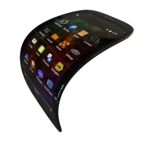
As more features are added to displays, this has created some material challenges – for example, adding touch functionality to a flexible screen (Figure 1). Traditional display materials such as ITO (indium tin oxide) have undesirable properties for this application, namely brittleness. This is a known problem with ITO coatings on PET films as they tend to produce micro-cracks when bent, which in turn lead to malfunctions and defects.
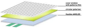
This material challenge led to the development of UV-curable conductive materials, including curable dielectric layers, which now have become standard in the industry (Figure 2).
Along with the development of UV-activated materials, radiation curing equipment also has advanced, with individual platforms now being integrated into one hybrid process.
The first platform is high-intensity excimer technology, which influences surfaces and their micro-characteristics. This allows functional films to take on additional features, such as anti-reflectivity, anti-static and anti-fingerprint marking.
Modern displays typically consist of nine layers of these high-tech functional films, which are assembled with a form of UV-activated adhesive. The adhesive is usually clear and not only provides a strong and lasting bond with desired optical properties, but also forms a protective seal against moisture while withstanding degradation from sunlight. These adhesives tend to be cured with LED and its respective UVA output.
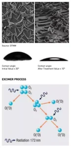
Prior to the bonding process, the surfaces need to be fully treated to ensure defect-free functionality. Mobile phones and tablets absorb a lot of mechanical wear, and the same is true of touchscreen displays. They need to be durable. For this reason, during production, the display is cleaned several times with excimer (172 nm). Excimer removes organic contaminants that would reduce adhesion and bond quality (Figure 3).
The excimer source is, in effect, a monochromatic UV (VUV, properly designated) source which produces high energy at 172 nm. The energy is sufficiently high to fracture bonds of organic compounds that are found as contaminants in the display production process. The fractured compounds, in turn, react with the ambient atmosphere with some useful effects. The particle removal rate increases with the energy level, although it is ultimately limited by the damage threshold of the material surface. It also should be noted that excimer is a cold technology – as it does not impart any thermal load onto the substrates that are being irradiated.
The energy potential of the 172 nm excimer is 7.23 eV, which is higher than many of the bonding energies of organic molecules, except carbon and oxygen. This sets up interesting reactions with the contaminants to produce ozone, water and carbon dioxide, which are easily removed to clean the surface. At this energy level, ozone and excited oxygen are generated and result in breaking bonds on the substrate. This improves adhesion and wettability, which are important for adhesives to cure within specification.
Once the films are cleaned and suitably activated for the next operation, the sister technologies of LED and UV are then utilized to complete the assembly.
LED and UV come into play
In this process, optical clear adhesives (OCA) generally are activated (cross-linked) using LED, which ensures good penetration and through cure. This allows the various layers of the display construction to be bonded together. The OCAs are formulated to deliver excellent optical properties (even in sunlight) with trouble-free and consistent dispensing properties which, together with the LED source, provide a reliable assembly operation.
Traditional UV systems, with mercury-doped bulbs, also are utilized to provide a high-energy UVC source. For display applications, this provides excellent scratch-, impact- and wear-resistance and also can enhance or embellish the surface finish.
These days, both UV and LED sources are well known and their strengths understood, but – as a point of interest – at this time, there is no (viable) replacement source for high-output UV arc lamps. UVC LEDs still are being developed, as the materials involved in producing UVC LEDs are very challenging from an output and stability perspective (and consequently, price).
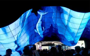
Due to the flexibility of the high-tech display films, they also are being used for interior and ambient lighting to add mood and other sensory inputs. As another example, traditional mirrors in vehicles are being replaced with cameras and their attending monitor displays (Figure 4).
The key to having all three technologies work effectively from one architecture lies in having exact process monitoring and control. Full integration of all three sources – excimer, LED and UV – have led to hybrid platforms being extensively used in other market sectors, such as flooring and furniture or soft-touch/haptics. The LED/UV duo also has been used for a number of years in the graphic arts industry, as has excimer/UV in converting. The point is that none of the radiation sources are new technologies; they simply are being combined with more process control as materials and media are developed for these radiation curing systems. Complex and intelligent application solutions require a seamless interaction.
As the hybrid application lexicon deepens, we see product examples such as flexible solar cells, batteries, sensors, intelligent lighting products, medical diagnostic (and drug delivery) devices, smart packaging and even clothing! And, based on current material trends, in the near future we will start to see more applications utilizing carbon nanotubes and graphene. In the mid-term, metamaterials, metallized glass and foam also will make an appearance, and true hybrid platforms will be an integral part of these leading-edge production processes.
Watch this space!
In his current position at IST Metz GmbH & Co Kg, Arnd Riekenbrauck focuses on new markets and application development for UV/LED/excimer technologies. A graduated engineer in printing technologies, he also holds a masters degree in economics and has been with IST for the last 17 years.
Chris Davis is head of sales – web and industrial systems at IST America. A degreed mechanical engineer, he joined the industry in 1993, driving narrow- and mid-web press sales until 2015 when he joined IST. Areas of expertise include printing, converting and industrial applications. For more information, contact Davis at 630.561.2024 or chris.davis@usa.ist-uv.com.


