



In the preceding column, I compared the feature size and print area of the principal UV vat printing technologies from large to small and their relevance to commercial applications. 1 This column reviews current and future applications of the additive manufacturing of ceramic materials as critical components in electronic devices, an industry in which small feature size is … [Read more...] about Additive Manufacturing for Electronics Applications
Additive Manufacturing
A New Chapter for PAMA: Strengthening the Future of Photopolymer Additive Manufacturing

As I step into the role of chair of the Board for the Photopolymer Additive Manufacturing Alliance (PAMA), I find myself reflecting on the exciting opportunities that lie ahead for both PAMA and the photopolymer additive manufacturing industry. It’s a transitional time in the 3D-printing sector, full of challenges and opportunities. I am both honored and humbled to lead PAMA … [Read more...] about A New Chapter for PAMA: Strengthening the Future of Photopolymer Additive Manufacturing
Additive Manufacturing Conference Review, Part 2
This column is a continuation of the Rapid+TCT Conference review. The previous column focused on panel discussions and presentations by leaders in the additive industry, with an emphasis on the current state and future trajectory of the industry. This column is focused on one-on-one conversations with materials suppliers and printer vendors, transitioning from strategy at … [Read more...] about Additive Manufacturing Conference Review, Part 2
Sustainable Raw Materials in Additive Manufacturing

By Corey Long and Clémentine Champagne, Arkema Additive manufacturing generally is considered to be a more environmentally responsible technology by enabling on-demand, local production, with the potential to reduce material waste and minimize the logistic footprint. The key to unlocking its full potential lies in the use of more sustainable raw materials. These innovations … [Read more...] about Sustainable Raw Materials in Additive Manufacturing
Photo-Rheology and FTIR Cure Analysis of Photopolymer Resins for Additive Manufacturing
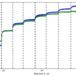
By Nicholas Gripp, Applied Molecules LLC This study undertakes a comprehensive examination of the photopolymerization kinetics of materials commonly used in additive manufacturing, focusing on the discernment of gel point vs. cure point. Leveraging the sensitivity of photo-rheology, 1 the onset of gelation is precisely identified, marking the transition from viscous to elastic … [Read more...] about Photo-Rheology and FTIR Cure Analysis of Photopolymer Resins for Additive Manufacturing