



In the preceding column, I compared the feature size and print area of the principal UV vat printing technologies from large to small and their relevance to commercial applications. 1 This column reviews current and future applications of the additive manufacturing of ceramic materials as critical components in electronic devices, an industry in which small feature size is … [Read more...] about Additive Manufacturing for Electronics Applications
Electronics
Automation for Photopolymer Optimization: Developments Toward Next-Generation Energy Materials

By Aldair E. Gongora and Johanna J. Schwartz, Lawrence Livermore National Laboratory Photopolymer synthesis and formulations optimization are areas with huge design complexity. Factors such as chemical composition, additives and fillers, absorption properties, cure kinetics and so on dictate the overall performance and lifetime of the photopolymer toward end-use applications. … [Read more...] about Automation for Photopolymer Optimization: Developments Toward Next-Generation Energy Materials
A New Class of UV-Curable Binders for Battery Applications
By Gary Sigel, Dan Baumann, Oliver Hamann, Pam Abbott, Donovan Hensley, Miltec UV, Inc. UV-based binders for lithium-ion (Li-ion) battery applications from Miltec first appeared in the literature as early as 2009 as a demonstrated “Environmentally Green Technology.” These UV binders did not contain the hazardous material NMP (N-methyl-2-pyrrolidone), which poses a significant … [Read more...] about A New Class of UV-Curable Binders for Battery Applications
Electrons In, Electrons Out: Electron Beam for Battery Production
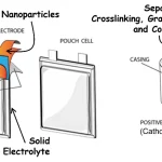
By Zhijia Du, Oak Ridge National Laboratory, and Sage Schissel, PCT Ebeam and Integration, LLC It is no secret batteries have become intrinsic to everyday life. Batteries have made mobile technology possible – from the flashlight to the Walkman to the cell phone – and, in turn, technology has demanded battery development keep pace. As batteries become more compact, powerful … [Read more...] about Electrons In, Electrons Out: Electron Beam for Battery Production
Hot Lithography: High-Precision 3D Printing of Flame-Retardant Photopolymers for the Electronics Industry
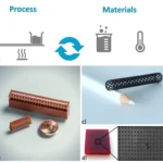
By Christian Frank, Kristina Hager, Reka Csizmadia, Markus Kury and Christian Gorsche, Cubicure GmbH Additive manufacturing (AM) has gained wide acceptance in R&D departments of companies in major industries (e.g., mobility, electronics, medical, aerospace, tooling) and their strategic initiatives toward industrial production solutions greatly contribute to the AM … [Read more...] about Hot Lithography: High-Precision 3D Printing of Flame-Retardant Photopolymers for the Electronics Industry